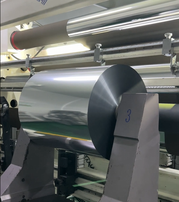
Copper Metallized PET Film for Circuit Patterns
Oct 19,2026 | FOSHAN CAILONG METALLIC PACKAGING MATERIAL CO.,LTD
Copper Metallized PET Film needs a different evaluation when the customer wants patterned electrodes rather than a continuous conductive sheet. The starting roll may conduct across its surface, yet the converted part still needs isolated features, intact traces and reliable connection areas. Those requirements determine whether the material is a useful candidate for the proposed circuit pattern.
Cailong's film portfolio lists its copper-coated PET product for electrode circuits, conductive tape and electromagnetic shielding. The published description confirms a polymer carrier with a deposited copper surface. It does not establish a minimum line width, a qualified patterning chemistry or an allowable circuit current. A converter should treat patterned-electrode development as a specific application trial rather than inherit approval from a general conductive-film description.
Draw the electrical features before choosing a route
Begin with a drawing that distinguishes conductive areas from insulating gaps. Mark connection pads, narrow transitions and any regions expected to bend. The drawing should show which features must remain electrically common and which must be isolated. This prevents a discussion about attractive copper coverage from overlooking the actual function of the finished part.
A broad electrode and a narrow power trace impose different requirements. The proposed use may need only sensing continuity, or it may need a defined current path. Establish that role before comparing the deposited metal with copper foil. A thin metallized carrier cannot be assumed to replace a conventional flexible circuit laminate solely because both contain copper.
Separate the carrier from the conductor
The PET substrate supplies the flexible support, while the deposited copper provides the conductive surface. Cutting the substrate changes the mechanical outline. Removing or interrupting copper changes the electrical pattern. These are different operations, and the required sequence depends on the intended design. A die-cut outline alone will not create every internal insulating gap shown in a circuit drawing.
Ask the patterning specialist whether the proposal uses selective deposition, removal of deposited metal, or assembly of separate conductive pieces. The product page does not qualify one of these routes. Choose a process with the supplier and converter, then verify that it produces both the intended geometry and a usable carrier. Avoid selecting a chemical or thermal process from the metal name alone.
Check the smallest meaningful feature
Large areas can look continuous while a narrow section contains an open path. Conversely, a fine bridge across an intended gap may be difficult to see but electrically significant. Incoming inspection of the unpatterned roll cannot resolve either issue. The finished feature geometry needs its own electrical acceptance criteria and inspection method.
Use a development pattern containing the demanding line, gap and connection-pad shapes from the real design. Include changes in direction and transitions between wide and narrow regions. These features can reveal weaknesses that a simple rectangular test coupon misses. Keep the sample layout tied to its position and orientation on the original web so the converter can investigate any repeated location-dependent result.
Inspect insulation gaps as carefully as traces
An isolated electrode requires a suitable gap, not merely reduced conductivity between two points. Check that the patterning process leaves the gap consistent and does not introduce debris or a residual conductive path. The correct test depends on the circuit's operating conditions and sensitivity. Define it with the electronics engineer before accepting a visual inspection as sufficient.
The PET surface exposed within a gap may also encounter adhesive, cleaning or assembly contact. A later coating can change the electrical environment even if the initial pattern passes. Assess the intended finished stack, including any cover or mounting layer. A reliable electrode layout is a property of that converted construction, rather than the appearance of bare patterned film.
Keep attachment and current limits explicit
The connection area must transfer the signal or current into the patterned copper without losing contact during assembly. Contact adhesive, a pressure arrangement and another joining method place different demands on the surface. The website provides no universal soldering or joining qualification for this product. Confirm the proposed interface before exposing the thin film to an unverified attachment process.
Do not derive a current rating from a sheet-resistance statement without the necessary conductor geometry, metal specification and thermal assessment. The substrate and surrounding layers influence how the part handles heating. If the application carries appreciable current, request data appropriate to that role and involve the circuit designer. A successful continuity check is only the starting electrical measurement.
Test the pattern after its real mechanical treatment
A flexible carrier is not proof that every patterned feature survives the same bending path. Locate bends relative to traces and contact pads, then reproduce the intended assembly motion. Compare electrical behavior before and after that treatment. The trial should identify whether any change occurs at the connection, a narrow feature or the broader conductive area.
If the part is bonded to a rigid support, assess the bonded configuration too. A trace that survives loose handling may experience a different strain near an attachment edge. Conversely, a support may limit movement in the finished assembly. Match the trial to the actual mechanical role rather than apply an arbitrary flex test and interpret it as a general lifetime claim.
Evaluate the complete patterning yield
Material replacement can change several costs at once: carrier handling, pattern formation, inspection and rejected parts. No cost reduction is established by the copper-coated web alone. Compare usable patterned parts produced by the chosen route, including the electrical inspection needed to release them. That is a more meaningful basis than comparing roll price with a different circuit material.
For a copper metallized PET project, provide the electrode drawing, intended electrical role, connection design and proposed patterning route. Identify the smallest line and gap, any bending region and the final supporting layers. These inputs let the material supplier and converter judge whether a trial is technically sensible and which feature should determine acceptance before larger-scale production is considered.
Comment