<section class="cat-desc">
<h2>Copper Metallized PET Film (Vacuum-Deposited Copper on BOPET / VMPET‑Cu)</h2>
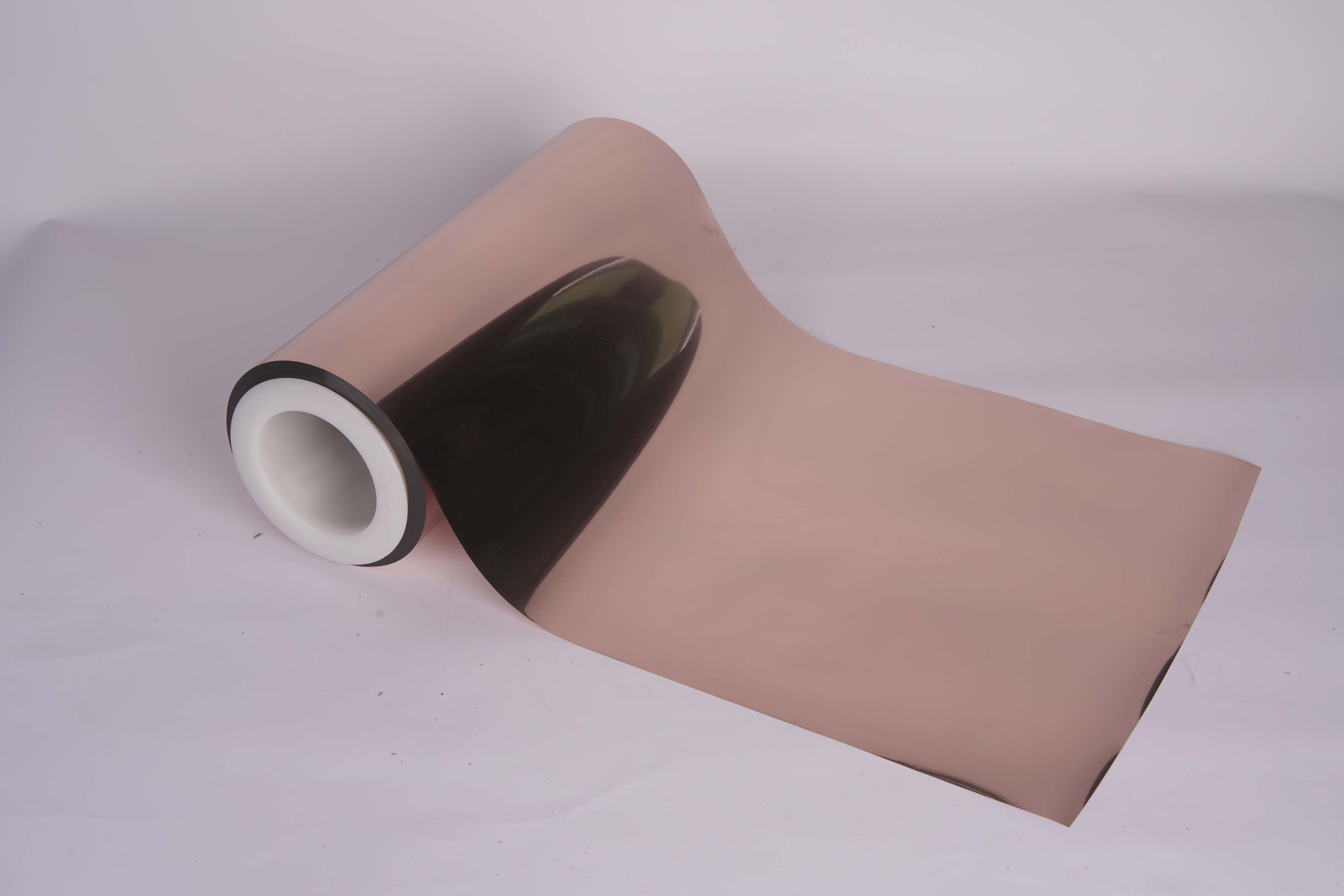
<p>
CaiLong <strong>Copper Metallized PET Film</strong> (also referred to as <em>polyester copper-coated film / VMPET‑Cu / vacuum silver‑copper film on BOPET</em>) is produced by depositing a high‑purity copper layer onto performance‑stable flexible PET (BOPET) substrates using roll‑to‑roll <strong>PVD / vacuum deposition</strong> technology.
The result is a functional conductive film that combines <strong>metal-level electrical & thermal conductivity</strong> with the <strong>dimensional stability, flexibility and processability</strong> of polyester film.
</p>
<h3>What makes it different from standard aluminum‑metallized films</h3>
<ul>
<li><strong>Higher bulk conductivity (Cu)</strong> — supports EMI shielding paths, grounding/static drain and conductive trace/heater-path concepts where Al layer resistance may be marginal.</li>
<li><strong>Uniform, well‑controlled Cu deposition</strong> — engineered for longitudinal/transverse coating uniformity and stable surface resistivity across the web.</li>
<li><strong>Strong metallization adhesion</strong> — copper layer adhesion optimized for downstream slitting, laminating, coating, die‑cutting or taping operations (testable per EAA or cross‑hatch methods per structure).</li>
<li><strong>Thermal & mechanical stability</strong> — retains PET’s tensile/stiffness/dimensional behavior while adding a robust metallic surface (suitable for heat, friction and repeated handling in industrial converting).</li>
</ul>
<h3>Typical specifications / capabilities (inquiry‑driven)</h3>
<ul>
<li><strong>Base substrate:</strong> BOPET (commonly); BOPI/other high‑performance webs available for special grades</li>
<li><strong>Product width:</strong> up to ≈2,100 mm (custom slit‑to‑width supported)</li>
<li><strong>Film thickness (PET substrate):</strong> can be specified across common industrial gauges (e.g. ≈12–188 µm depending on grade/structure)</li>
<li><strong>Cu surface resistivity:</strong> controllable per design (including low‑ohm/sq targets for shielding/conductive applications)</li>
<li><strong>Finish / color:</strong> characteristic metallic copper tone; optional protective/top‑coat or nickel‑flash concepts discussed case‑by‑case</li>
<li><strong>Processing note:</strong> Cu surfaces can oxidize under certain storage/exposure conditions — packing, humidity control and optional surface protection schemes are part of how we stabilize shipments</li>
</ul>
<h3>Key application fields</h3>
<ul>
<li><strong>EMI/RFI shielding & grounding:</strong> flexible shields, wrapped shields, conductive laminates, equipment interiors</li>
<li><strong>Electronic materials: