
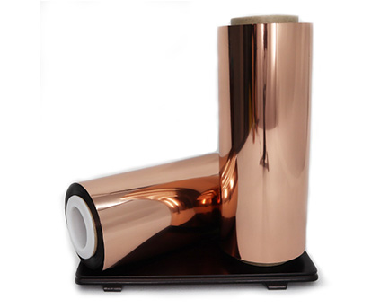
Vacuum Deposited Copper Film: The Ultra-Thin, All-in-One Conductor Powering the Flexible Electronics Revolution Introduction
Jun 04,2026 | FOSHAN CAILONG METALLIC PACKAGING MATERIAL CO.,LTD
The relentless drive toward miniaturization and functional integration in modern electronics presents a core dilemma for engineers and designers: how to achieve efficient signal transmission, thermal management, and electromagnetic compatibility within ever-shrinking spaces. Traditional solutions often involve stacking multiple materials, leading to bulky, complex, and costly designs. Vacuum Deposited Copper Film emerges as the innovative material that solves this puzzle. By applying an atomically-thin, high-purity copper layer onto ultra-thin, flexible substrates like BOPET or BOPI via advanced Physical Vapor Deposition (PVD) technology, it creates a versatile "all-in-one" material that combines superior conductivity, thermal dissipation, shielding, and flexibility. This material is quietly revolutionizing everything from consumer gadgets to cutting-edge technology.

Part 1: Core Technology Breakdown: How Precision and Purity Create Excellence
The exceptional performance of Vacuum Deposited Copper Film is rooted in its precise, state-of-the-art manufacturing process. Understanding this process is key to appreciating its value.
-
Substrate Selection: The Foundation of Performance
-
BOPET (Polyester Film): The preferred choice for most applications due to its excellent mechanical strength, dimensional stability, chemical resistance, and cost-effectiveness. It withstands standard surface treatments (like corona or coating) and soldering temperatures, making it ideal for flexible circuits and shielding.
-
BOPI (Polyimide Film): The "premium" choice for high-performance applications. It offers long-term thermal stability exceeding 200°C, exceptional electrical insulation, and outstanding dimensional stability. It is the perfect substrate for aerospace, automotive electronics, or flexible circuits requiring high-temperature soldering.
-

-
Core Process: Physical Vapor Deposition (PVD)
Inside a high-vacuum, roll-to-roll coater, a source of 99.999% pure copper (typically wires or a target) is energized by an electron beam or magnetron sputtering. This causes copper atoms to vaporize. In the vacuum chamber, these pure copper particles travel linearly and condense uniformly onto the moving substrate, forming a nano-to-micron thin metallic layer. The precision of this process determines the coating's adhesion, uniformity, purity, and resistivity.
-
The Birth of Performance Advantages
This atomic-level bonding creates a product that inherits the best properties of both metal and polymer:
-
Metallic Advantages: Gains copper's excellent electrical conductivity (low sheet resistance), thermal conductivity, high reflectivity, and electromagnetic shielding effectiveness.
-
Polymer Film Advantages: Retains the substrate's ultra-thin profile, lightweight nature, flexibility, high electrical insulation, chemical resistance, and dimensional stability.
-
Part 2: Why It's a Revolutionary Alternative to Traditional Materials
The advantages of Vacuum Deposited Copper Film become clear when compared to conventional solutions:
|
Feature |
Vacuum Deposited Copper Film |
Traditional Rolled/Electrodeposited Copper Foil |
Conductive Inks/Pastes |
|---|---|---|---|
|
Thickness & Weight |
Extremely thin (total <15µm possible), very light |
Relatively thick and heavy |
Coating is thin, but performance depends heavily on substrate |
|
Flexibility & Bend Endurance |
Excellent, can withstand thousands of dynamic flex cycles |
Fair, prone to fatigue and cracking with repeated bending |
Good, but the coating can develop micro-cracks |
|
Conductivity |
High (volume resistivity close to bulk copper) |
High |
Significantly lower, often by several orders of magnitude |
|
Patterning Precision |
Very high (can achieve micron-level lines via precise etching) |
High |
Lower, limited by printing resolution |
|
Process & Eco-Friendliness |
Dry PVD process, environmentally friendly; allows fine-line etching |
Traditional process, significant copper waste during etching |
Involves chemicals, may contain solvents |
|
Cost Consideration |
High material utilization, ideal for high-performance, precision apps |
Mature, but with higher material waste |
Suitable for simple graphics, low-cost applications |
Part 3: Diverse Application Scenarios: Empowering Modern Technology
Its unique property portfolio enables key solutions across multiple advanced fields:
-
Advanced Thermal Management Solutions
-
Ultra-Thin Vapor Chamber (VC) Substrate: Serves as the wick and wall material for ultra-thin VCs, enabling rapid 3D heat spreading for smartphone SoCs and 5G chips.
-
Flexible Thermal Interface Materials: Conforms to irregular surfaces between chips and housings, efficiently drawing heat away without adding structural burden.
-
-
High-Frequency & High-Speed Signal Transmission
-
Fine-Line Flexible Printed Circuits (FPCs): Especially critical for applications demanding high flexibility and reliability, such as circuits in foldable phone hinges, automotive dynamic camera cables, and medical endoscopes.
-
Millimeter-Wave Antennas: Used as antenna radiators or transmission lines in 5G/6G devices and automotive radar, offering low loss and easy conformal design.
-
-
Electromagnetic Compatibility (EMC) Assurance
-
Comprehensive EMI Shielding:
-
In-Mold Labeling (IML) Shielding: Patterned decorative shielding films are molded directly onto plastic housing interiors, combining aesthetics with function.
-
Conductive Tapes & Gaskets: Provide lightweight solutions for gap shielding and grounding.
-
Shielding Wrap: Used to bundle FPC cables, preventing signal crosstalk.
-
-
-
IoT & Smart Packaging
-
High-Performance RFID Tag Antennas: Offers better conductivity and longer read range than etched aluminum antennas, and superior stability compared to printed antennas—ideal for high-end logistics and asset management.
-
NFC & Wireless Charging Coils: Enables slim form factors for device identification, interactive marketing, and wireless power receivers.
-
-
New Energy & Frontier Technologies
-
Flexible Battery & Sensor Electrodes: Provides a flexible, potentially biocompatible (when treated) conductive base for wearable health monitors and e-skin.
-
Photovoltaics: Can be used in conductive grids or backsheets for certain types of flexible solar cells.
-
Part 4: Future Outlook: Toward a Smarter, More Integrated Era
As wearable devices, flexible displays, biomedical electronics, and the Internet of Things (IoT) evolve, demands on conductive films will grow: thinner, more flexible, and more functionally integrated. The next evolution for Vacuum Deposited Copper Film may include:
-
Multi-Functional Integration: Stacking additional functional layers (e.g., insulation, protection, optical layers) atop the copper to create "systems on a film."
-
Structural & Patterning Innovation: Developing 3D structured copper deposition and selective area deposition for differentiated performance.
-
Sustainability: Enhancing substrate recyclability or developing copper deposition on bio-based, degradable films.

In summary, Vacuum Deposited Copper Film is not merely a material substitute; it is an enabling technology that redefines product design paradigms. It integrates the once-separate functions of conduction, heat dissipation, shielding, and structural support into a single film thinner than a human hair, granting engineers unprecedented design freedom and space efficiency. From the heat spreader ensuring your smartphone's smooth performance, to the stable signal transmission in an electric vehicle's battery system, to the anti-counterfeit label on a premium product, Vacuum Deposited Copper Film supports the reliable operation of our connected world with its invisible yet powerful presence. For innovators crafting the next generation of electronics, deeply understanding and utilizing this material is a critical step toward securing a competitive future.
Comment


